Hiden Analytical have been designing and developing the highest quality quadrupole mass spectrometer based systems for over 40 years. We have built a reputation for delivering instruments with superior sensitivity, accuracy and reproducibility together with a first class global service and applications support network.
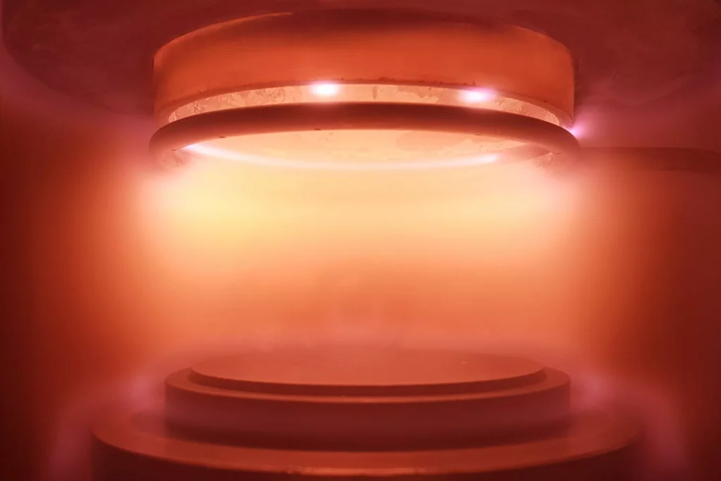
Thin film processing in research, development and functionalisation of surfaces has a broad application range in microelectronics, nanotechnology, photovoltaics, mechanics, optics, photonics, textiles, coatings, chemistry, biology and medicine.
Thin film processing utilises a wide range of techniques, including:
- Magnetron sputtering
- ALD – Atomic Layer Deposition
- CVD – Chemical Vapour Deposition
- MOCVD – Metal Organic Chemical Vapour Deposition
- PECVD – Plasma Enhanced Chemical Vapour Deposition
- MBE – Molecular Beam Epitaxial growth
- RIE – Reactive Ion Etch
- IBE/RIBE – Ion Beam Etch and Reactive Ion Beam Etch
Each technique is often tailored for a specific application, requiring special process parameters to produce the surface/film properties required. Hiden mass spectrometers provide critical insight into thin film processing and characterisation enabling optimisation of thin film production and surface quality.
Hiden systems are individually configured to ensure optimum analyser response for sensitivity and speed.
To see the systems used in this field, please visit the link below: